Metals are good conductors of electricity. Insulators are bad conductors of electricity. Similarly, semiconductor devices are partial conductors of electricity means their conductivity lies between conductors and insulators.
Let’s discuss about the Fermi level first. Fermi level is the energy level taken up by an electron at the temperature range of zero Kelvin. So, at the temperature of zero Kelvin the energy levels which are lower than i.e. below the Fermi level are filled completely by electrons. When we will provide energy to the electrons then they will absorb energy one by one and will excite to higher energy levels. This is clear that the electrons which are present at larger distances from the nucleus will not be much affected by the stronger nuclear forces. So, in other words we can say that these electrons are relatively free as compared to the other electrons. The classification of these materials as solids, metals and insulators is according to the positioning of the conduction as well as the valence bands.
Metals: In case of metals, electrons fill the conduction band partially. The overlapping of both the bands i.e. valence and conduction band also take place. This shows that no forbidden energy gap is present. The diagram is shown below:
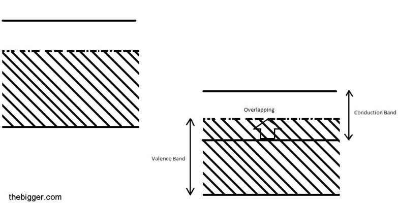
Those electrons which are present below the fermi level are capable of gaining energy from some outer source and can shift to the higher energy levels above the Fermi level i.e. in the conduction band. Then these electrons will behave as free electrons. Due to the presence of these free electrons the metals behave as good conductor of electricity. When small amount of electric field is applied to the metals then the electron movement will start in the direction opposite to that of the electric field. This electron movement results in the generation of the current.
Insulators: In case of insulators the forbidden energy gap is extremely high as compared to the conductors. On the other hand its valence band is fully filled with the electrons, whereas its conduction band is empty. Let’s take example of diamond. The approximate value of forbidden energy gap for diamond is nearly 6eV. As we have discussed above that the valence band is filled fully with electrons. Using the concept of Pauli’s exclusion principle, no electrons will be free. So, electrons will not be able to reach the conduction band. Hence these materials act as insulators due to the absence of electrical conductance.
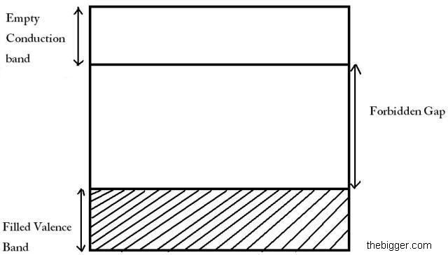
Semiconductors: In case of semiconductors the conduction band is empty and the valence band is fully filled with electrons. Like insulators, forbidden energy gap is not so large in case of semi conductors. The energy gap is very small. This energy gap is nearly of 1eV. For different products this energy gap is different. E.g. For silicon and germanium this energy gap is nearly 1.1eV and 0.72eV respectively.
If the temperature will be zero Kelvin then it is impossible for the electrons to cover this energy gap of 1eV. No electron will jump to the conduction band. Hence no conductivity will take place. It is clear that at the temperature range of zero Kelvin these substances act as insulators. But if these substances are placed at room temperature then the electrons will gain some amount of thermal energy and will shift to the conduction band. When these electrons reach the conduction band then these are free to move. Then they will start showing conductivity when some electric field is applied. In other words, we can say that at room temperature these substances will show some amount of conductivity.