Those semi conductors in which impurities are missing are known as intrinsic semiconductors. The electrical conductivity of the semiconductor depends upon the total no of electrons shifted to the conduction band from the valence band. This phenomenon is called as intrinsic conductivity.
The most common examples of the intrinsic semiconductors are silicon and germanium. Both these semi conductors are used frequently in manufacturing of transistors and electronic products manufacturing. The electronic configuration of both these semiconductors is shown below:
Germanium -1s22s22p63s23p6 3d104s24p2
Silicon: 1s2 2s2 2p6 3s2 3p2
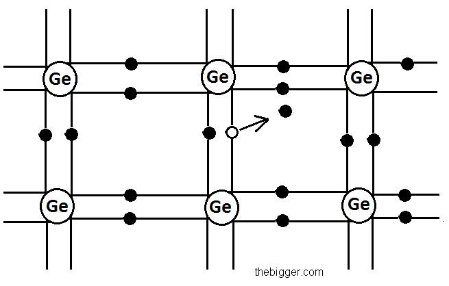
In the electronic configuration of both the semiconductor crystals there are four valence electrons. These four electrons will form covalent bonds, with the neighboring electrons of the germanium atoms. Each covalent bond is formed by sharing each electron from the each atom. After bond formation, no free electron will remain in the outermost shell of the germanium semi conductor.
The figure of germanium structure is shown below:
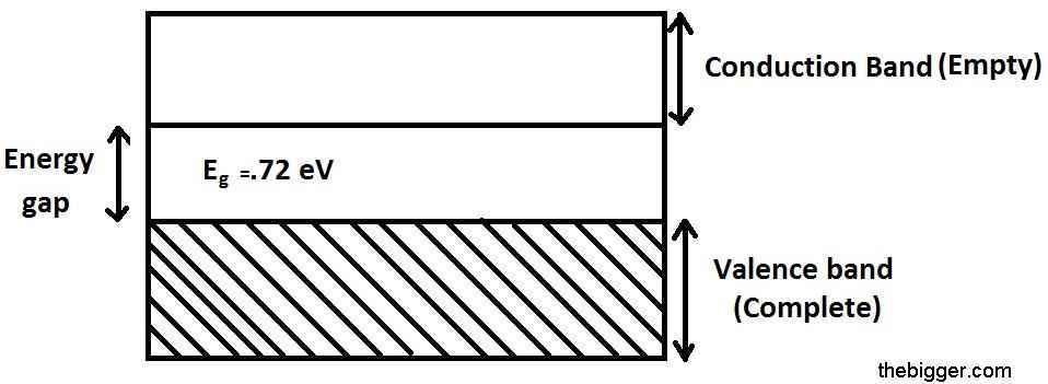
If the temperature will be maintained at zero Kelvin, then the valence band will be full of electrons. Energy gap is nearly 0.72 eV for germanium. So, at such a low temperature range it is impossible to cross the energy barrier. It will act as an insulator at zero Kelvin. Electrical conduction starts only if there is breakage in the covalent bonds and some of the electrons become free to jump from valence band to the conduction band. The minimum energy required to the break the covalent bond in germanium crystal is 0.72 eV and for silicon its value is 1.1 eV.
But if these semi conductors are placed at room temperature then the thermal energy generated at room temperature will help to excite some electrons present in valence electrons to shift to the conduction band. So, the semi conductor will be able to show some electrical conductivity. As the temperature increases, the shifting of the electrons from the valence band to the conduction band will also increase. The holes will be left behind in the valence band in place of electrons. This vacancy created by the electron after the breakage of the covalent bonding is known as hole. Holes are shown in the figure given below. Hollow circles in the figure are representing the holes.
When this semi conductor is placed under the influence of electric field then the holes movement and the electron movement will be opposite to each other. During this whole process the no of holes and the free electrons in the circuit of the intrinsic semi conductor will be same.
Equation between the density of free electrons, density of holes and the density of the semiconductor is shown below:
ne = nh = ni
n e and n h in the above equation are the number densities of free electrons and no density of holes respectively. Similarly, ni is the intrinsic density of the carriers i.e. the holes and free electrons.
Formula which can be used to calculate the no of holes and the electrons in the semi conductor is given by:
ne=nh= AT3/2e-Eg / 2kT
As we have discussed above that when we will increase the temperature the no of electrons as well as the holes will increase.
Conclusion: It is very difficult task to make an intrinsic semiconductor because we can’t use highly pure materials for constructing the semi conductors.