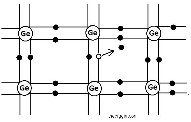
To clarify this concept, let’s consider the crystal structure of any of the semiconductor. Now lets take the example of germanium crystal. In germanium crystal covalent bonding is present between its various atoms. In the diagram shown below the crystal is looking like a two dimensional structure. But in actual it is having a three dimensional structure. In this atoms are present at tetrahedral angles. When the electrons present in the atoms making covalent bonds with each other, will receive some amount of energy then it will lead to the breakage of the covalent bond. Then one of the electrons from the covalent bond will be able to move freely along the whole crystal lattice. After moving from its place it will leave a vacant space behind. Now electron from the hole is missing and that hole will be having an equal amount of positive charge to that of the electron. Similarly, new bond breakage can take place and the created hole can attract the electrons of the broken covalent bond. So, as a result the covalent bond will be completed again and a new hole will be created at some other place in the crystal lattice. From the structure of the figure shown below it is clear that the electron can come to complete the covalent bond from any of the four atoms.